In-situ Nanometrology
![]() Operando XPS
Operando XPS
We systematically develop and apply in-situ metrology to probe and understand the atomic level mechanisms that govern the growth and device behaviour of nanomaterials in realistic process environments. We thereby explore a wide range of techniques, incl. high-pressure XPS, in-situ XRD, environmental TEM and SEM, in-situ STM and in-situ optical spectroscopy. We aim at correlative probing at industrially relevant process conditions and explore additional degrees of freedom via MEMS type holder designs.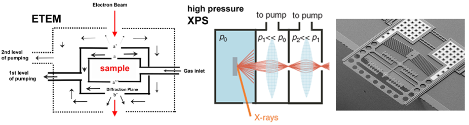
We recently developed and installed a near ambient pressure (NAP) X-ray photoemission spectroscopy (XPS) system is for high-throughput chemical surface analysis under application-relevant environmental conditions. This user facility is part of the Henry Royce Institute at Cambridge and please see the facility web page regarding access.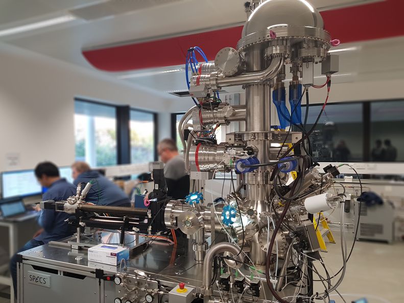
In collaboration with:
Dr F. Ross (IBM)
Prof. R. Schloegl (FHI, Germany)
Dr C. Cepek, Dr C. Africh (CNR, Italy)
Prof. J. Baumberg (Physics, University of Cambridge)
References:
Panciera et al. Nature Comm. 7, 12271 (2016)
Di Martino et al. Nano Lett. 15, 7452 (2015)
Weatherup et al. JACS 136, 13698 (2014)
Patera et al. ACS Nano 7, 7901 (2013)
![]() Operando SEM
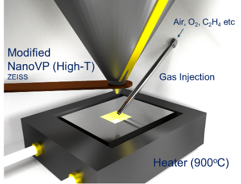
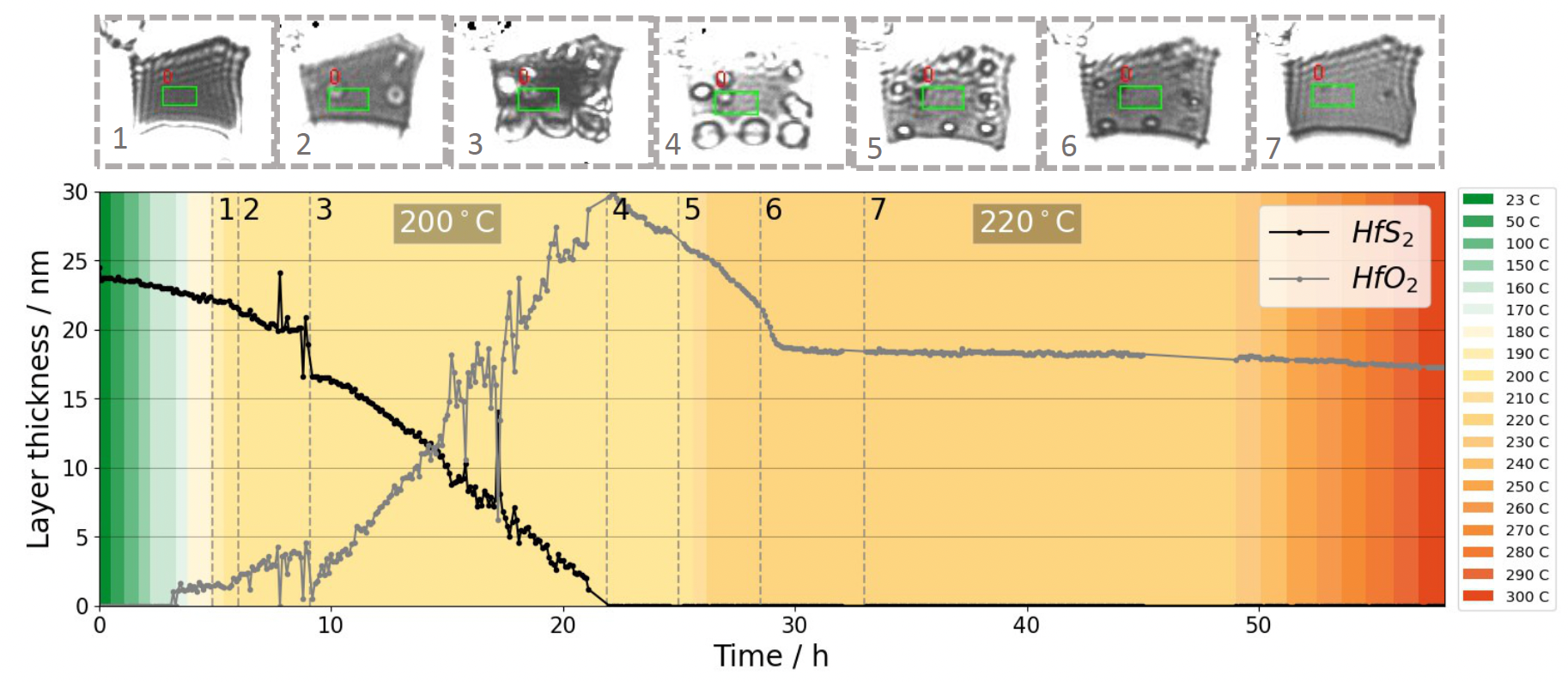
Operando SEM
Operando Scanning electron microscopy…
In collaboration with:
References:
![]() Optical Ellipsometry
Optical Ellipsometry
Optical ellipsometry is emerging as a powerful method for high-throughput materials characterization, applicable across a broad range of materials and contexts. This non-invasive optical technique measures changes in polarization as light reflects or transmits through a sample. In our group, we aim to harness the ellipsometer’s multiple measurement modes for exploring optical properties, in operando growth kinetics, and large-scale mapping of 2D materials. It is particularly distinguished as one of the few techniques capable of non-destructive characterization of buried layers and interfaces, effectively combining the benefits of optical microscopy and spectroscopic ellipsometry. For emergent 2D materials, atomic monolayer thickness resolution has been demonstrated on different substrates, and our methods can distinguish between mono-, bi-, and trilayer systems. Our research group is committed to streamlining this process, enhancing its efficiency, and applying it to tackle various challenges in the field of 2D materials.
In collaboration with:
References: