Research Themes
The ability to engineer device materials at a sub-100nm scale opens unmatched opportunities to tailor enhanced electrical, optical, magnetic and mechanical properties and functionalities that can be effectively integrated and combined into new form factors and technologies. In as much as integrated circuits and systems shaped our society over the last decades, integrated nanomaterials are set to have revolutionary impact on an ever increasing number of sectors, including information & communication technologies, healthcare, energy conversion and storage, security, transport and environmental technologies.
With the size of materials reduced to nm-size scale, their properties not only depend ever more closely on their detailed structure, size, shape and dimensionality but importantly also on their surfaces and interfaces. Much of the new functionality arises from the ability to combine an increasing diversity of materials and achieve greater structural complexity and more complex device architectures. This necessitates new growth and heterogeneous material integration strategies, and for nanomaterials bottom-up or self-assembly approaches are thereby of crucial importance. We investigate crystal growth of nanomaterials that is at the heart of all such emerging technology and is the key future enabler.
Towards High-throughput Experiments and Automation
The field of nanomaterials stands at a pivotal juncture, where the integration of high throughput experimentation, powered by robotics, and in-situ nanometrology, emerges as a pathway towards the rational design of novel materials for various applications. We intend to combine the elements our group has long gained experience and expertise in: in-situ characterization, growth, and implementation in devices. Traditionally, there has been a large and immutable, complexity and pressure/environment gap in nanomaterials research compared
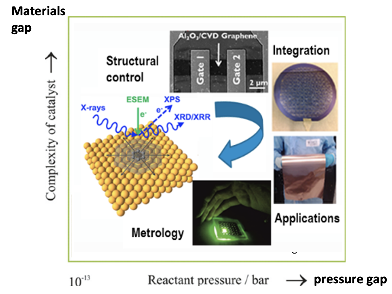
High throughput experimentation, when combined with robotics, offers a transformative approach to the discovery and optimization of nanomaterials. Robotics can automate the labor-intensive and time-consuming processes associated with the synthesis and characterization of nanomaterials, thereby significantly increasing the speed of experimentation. This automation also leads to higher reproducibility and precision in experiments, reducing human error and variability in results.
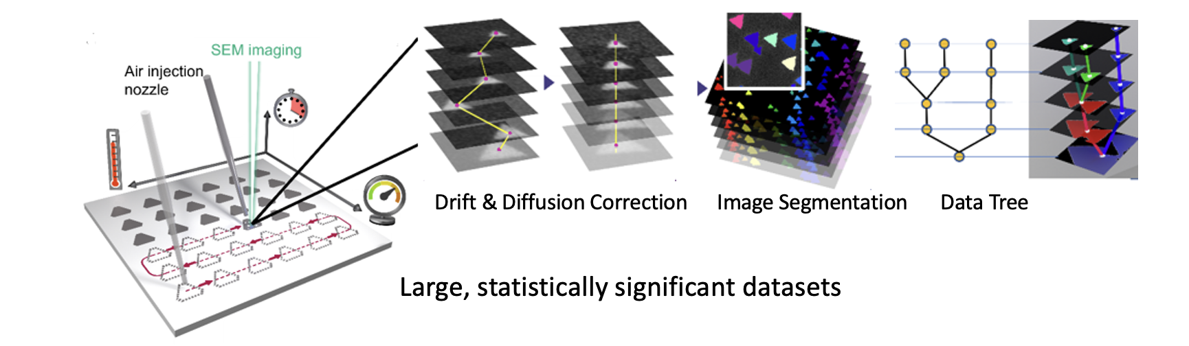
The role of in-situ nanometrology cannot be overstated in this context. It enables the real-time characterization of nanomaterials during their synthesis, providing immediate feedback that can be used to adjust experimental parameters on-the-fly. This capability is crucial for understanding the complex dynamics of nanomaterial growth and evolution, thereby allowing for the fine-tuning of properties at the nanoscale. In-situ techniques, such as electron microscopy and X-ray diffraction, can reveal insights into the atomic structure, morphology, and chemical composition of materials as they form, offering a window into the processes that govern material behavior at the nanoscale.
The integration of AI and machine learning (ML) techniques further amplifies the potential of this combined approach. AI algorithms can analyze vast datasets generated by high throughput experiments, identifying patterns and correlations that would be intractable for human researchers to discern. This analysis can guide the design of future experiments, predict material properties, and even suggest new materials compositions and configurations. By harnessing AI, we can move towards a more rational design of nanomaterials, where decisions are informed by data-driven insights rather than trial and error.